


Antminer S9K S9SE Hash Board Repair Guide
Version date: 2019.7.9
File Category: Maintenance Plan
Content of this Volume: It mainly describes the troubleshooting of various faults of S9K S9SE, and how to use the test tool for accurate positioning.
※ The copyright of this article belongs to Bitmaintech Pte.Ltd. (Bitmain). The article shall solely be reprinted, extracted or used in any other ways with the permission of the copyright owner. Please contact Bitmain official customer service if there is any need of reprinting or quoting.
I. Requirements on the Maintenance Platform
1. The constant temperature soldering iron (350-400°C). The tip soldering iron head is used for soldering chip resistors and capacitors.
2. The thermal chimney is used for chip disassembly and soldering, be careful not to heat for a long time to avoid PCB foaming.
3. APW3++ power supply (output 12V, 133A Max), used for test and measurement of the hash board.
4.The Fluke 15b+ multimeter, tweezers, S9k S9se test jig (if there is condition, an oscilloscope can be configured).
5. Flux, water for cleaning panel with anhydrous alcohol; water for cleaning panel is used to clean flux residue and appearance after maintenance.
6. Thermally conductive adhesive is used to re-attach the cooling fin after repair.
If you need to repair Antminer S9k S9se, in addition to the necessary tools mentioned above, you also need Universal test fixture, 862D desoldering station, Tin scraper and other efficient tools.
Of course, this choice may be more troublesome, you can also choose the convenient Bitmain Antminer hash board repair bundle.
II. Requirements on Maintenance Operations
1. The maintenance personnel must have certain electronic knowledge, more than one year of maintenance experience, and master QFN package welding technology.
2. After repair, the hash board must be tested twice and confirmed as OK before it can pass!
3. Pay attention to the operation method when replacing the chip. After replacing any accessories, the PCB board is not obviously deformed, and the replaced parts and the surrounding area shall be checked for whether there is open and short circuit.
4. Determine the maintenance station object and the corresponding test software parameters and test jigs.
5. Check whether the tools and jigs can work normally.
(Whether the power output is the same as the setting in the jig config file. Different BIN level and chip package mode need to correspond to the config and single-board-test files of the single board test jig program.)
III. Principle and Structure
1. Principle overview
1.1 S9K S9SE hash board is composed of 6 voltage domains connected in series. There are 10 BM1393 chips in each voltage domain, and there are 60 BM1393 chips on the whole board.
1.2 There are 208 cores on a single BM1393 chip, the domain voltage is 1.6V, and the total voltage of the 6 domains on the whole board is 9.6V-9.9V
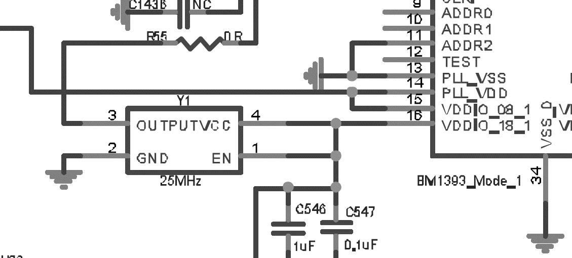
1.3 S9K S9SE clock is composed of two 25M active crystal oscillators (Y1, Y2), Y1 is transmitted from the first chip to the 30th chip in series, and Y2 is transmitted from the 31st chip to the 60th chip in series
1.4 There is independent small cooling fin on the front and back of each chip of the S9K S9SE hash board. The small cooling fin on the front side is the SMT patch, and the small cooling fin on the back side is fixed on the back of the IC by the thermally conductive adhesive after the initial measurement. After the repaired and replaced chip passes the test, it is necessary to evenly apply black thermally conductive adhesive on the IC surface and heat and fix it.
Note:
In the maintenance process, when replacing the circuit board components or the chip, in order to reduce the damage of high temperature of the blower gun to the PCB board and the chip, it is necessary to first remove the small cooling fins near the faulty component and on the back of the PCB board before replacing.
There are test points on the PCB chip surfaces. When manufacturing and repairing, if there is no cooling fin attached on the PCB chip, the test point on the chip surface can be used; for repair of finished products (after-sales repair), since the front and back of the PCB are covered by cooling fins, it needs to locate fault through the test point on the chip surface of the PCB. A special slender test lead can be used to probe the cooling fin gap for measurement. However, since the SMT small cooling fin is connected to the ground of each voltage domain, it is necessary to pay attention to the insulation of the test lead in measurement to avoid short circuit caused by the test lead.
2. Analysis of key point
2.1 The following figure shows the chip domain distribution, signal path and circuit distribution of the S9K S9SE signal board:
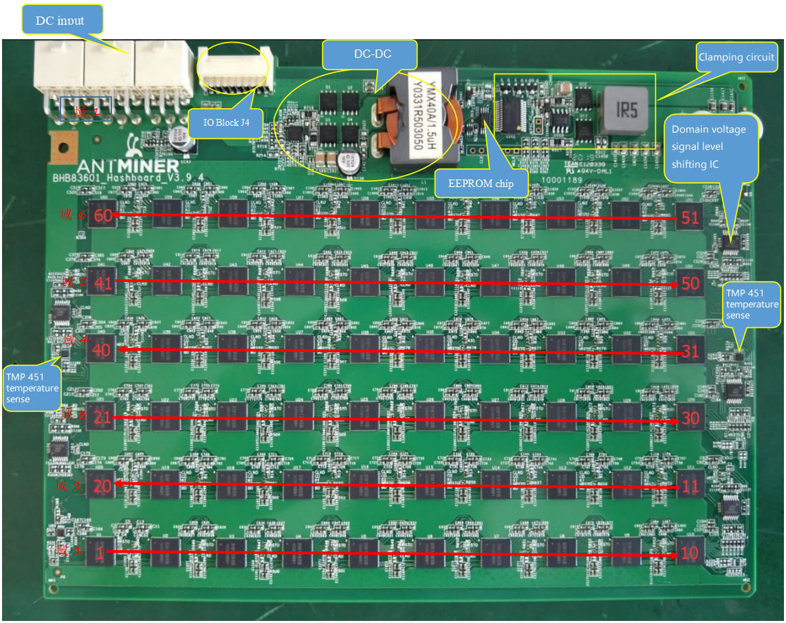
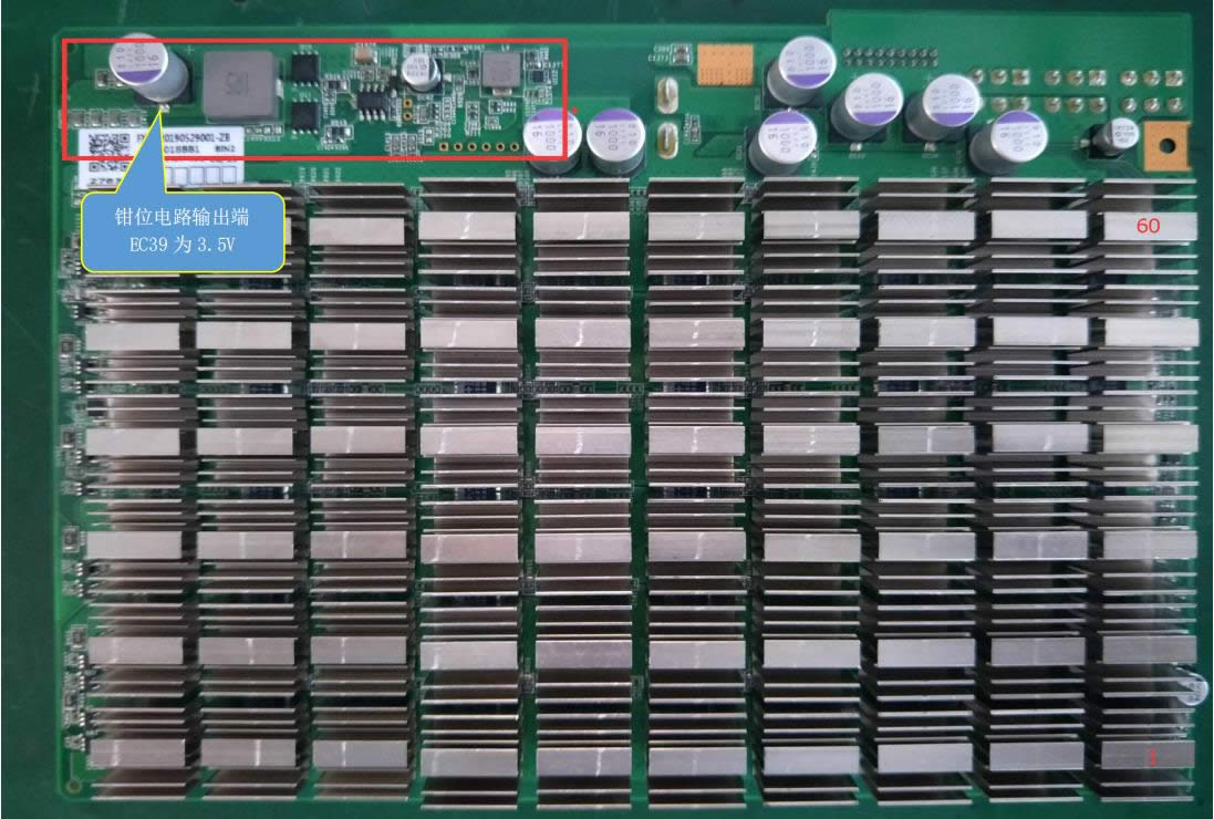
The flow direction of CLKO signal is generated by Y1 25M crystal oscillator, which is transmitted from chip U1 to chip U30; it is generated by Y2 25M crystal oscillator, and is transmitted from chip U31 to chip U60. When standby and computing, the voltage is 0.9V.
Signal CO (CI, C0) enters from the Pin 7 at port IO (J4), and is then transmitted from chip U1 to chip U60; when the IO line is not inserted, the voltage is 0, and the voltage is 1.8V when computing.
Signal RI (R1, RO) returns from chip U60 to chip U1, and then returns to the control board from the pin (J4) 8 at IO port; when the IO signal is not inserted, the voltage is 1.8V, and the voltage is 1.8V when computing.
Signal BO (BI, BO) flows from chip U1 to U60 to lower the level; the voltage is 0V when there is no IO line inserted and during standby, there is a pulse signal around 0.3 when computing, generally if no voltage can be measured, it is normal.
Signal NRSTO (NRSTO, NRSTI) enters from pin (J4)) 3 at IO port, and is then transmitted from chip U1 to chip U60; the voltage is 0V when there is no IO signal inserted and during standby, and the voltage is 1.8V when computing.
2.2 Key circuits of the S9K S9SE hash board
2.2.1 Schematic diagram of U122 power management
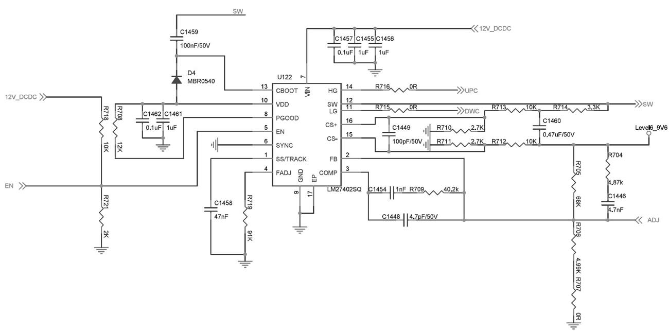
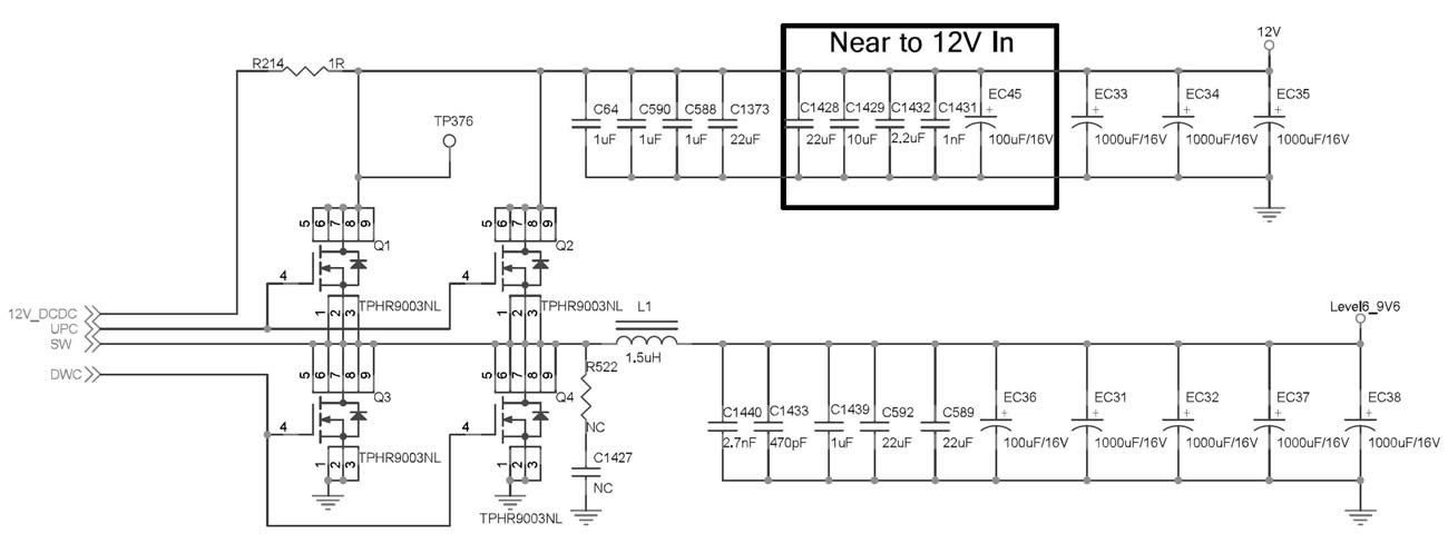
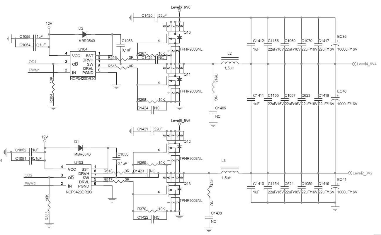
2.2.2 Schematic diagram of DC to DC circuit
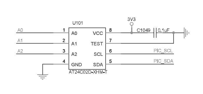
2.2.3 Schematic diagram of EEPROM IC (single board test will change the magic number, temperature sensing information and CRC information in the EEPROM)
2.2.4 Schematic diagram of clamping circuit
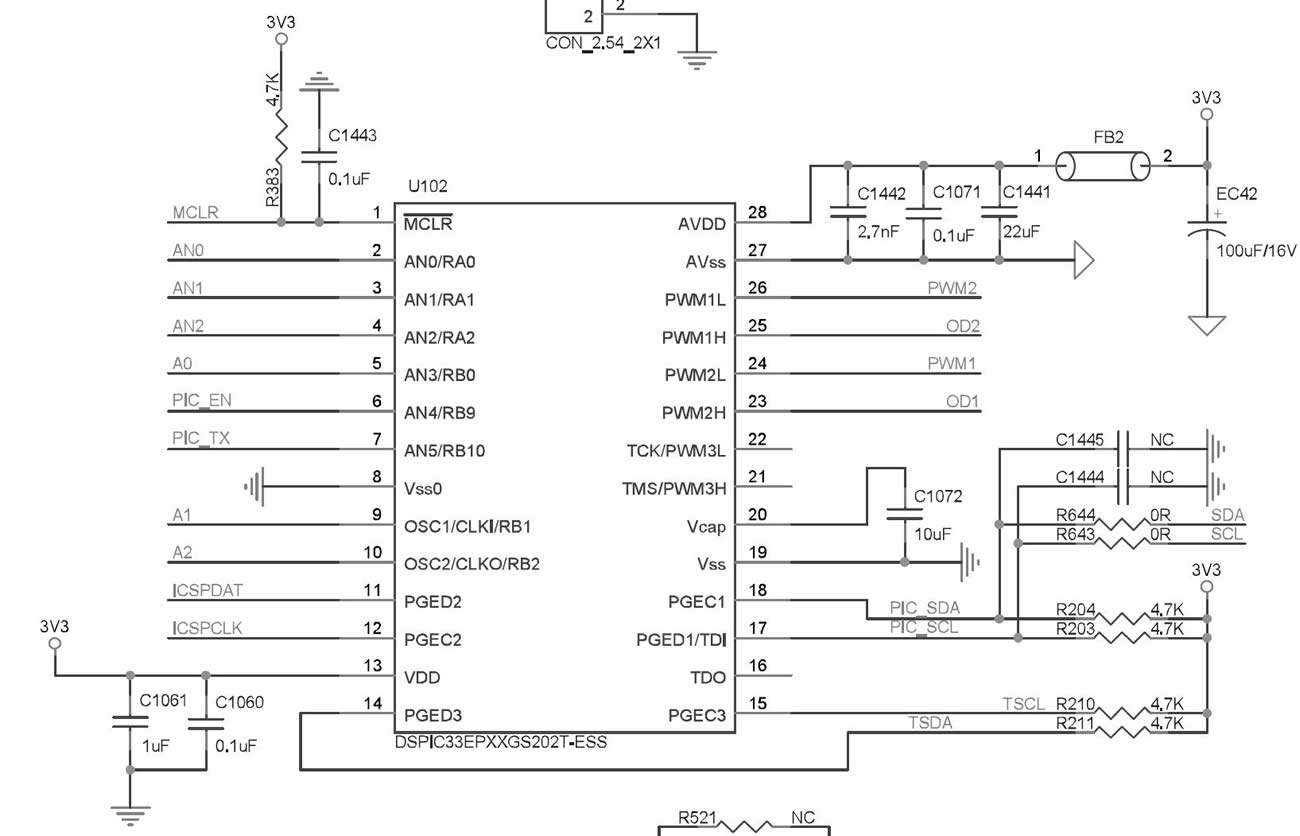
2.2.5 Schematic diagram of PIC U102
2.2.6 Signal test points of each chip (as shown below after amplified):
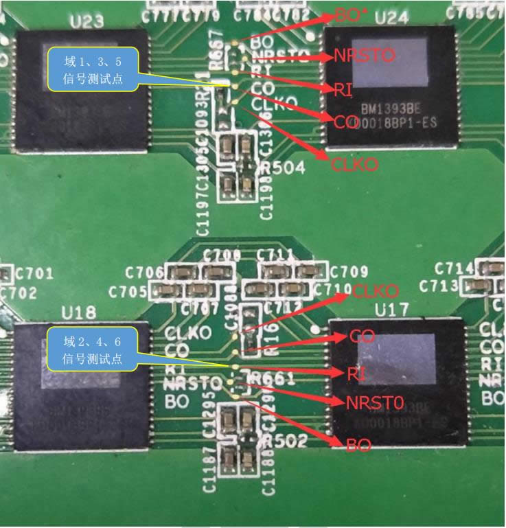
1. Signal test points in Domain 1, 3, 5
2. Signal test points in Domain 2, 4, 6
2.2.7 Pin circuit diagram of each chip in Domain 1, 3, and 5
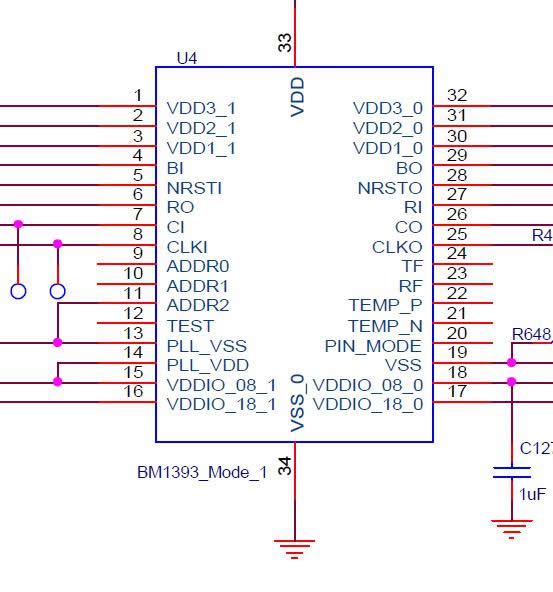
2.2.8 Pin circuit diagram of each chip in Domain 2, 4, and 6
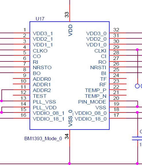
2.2.9 Circuit diagram of J4 at IO port
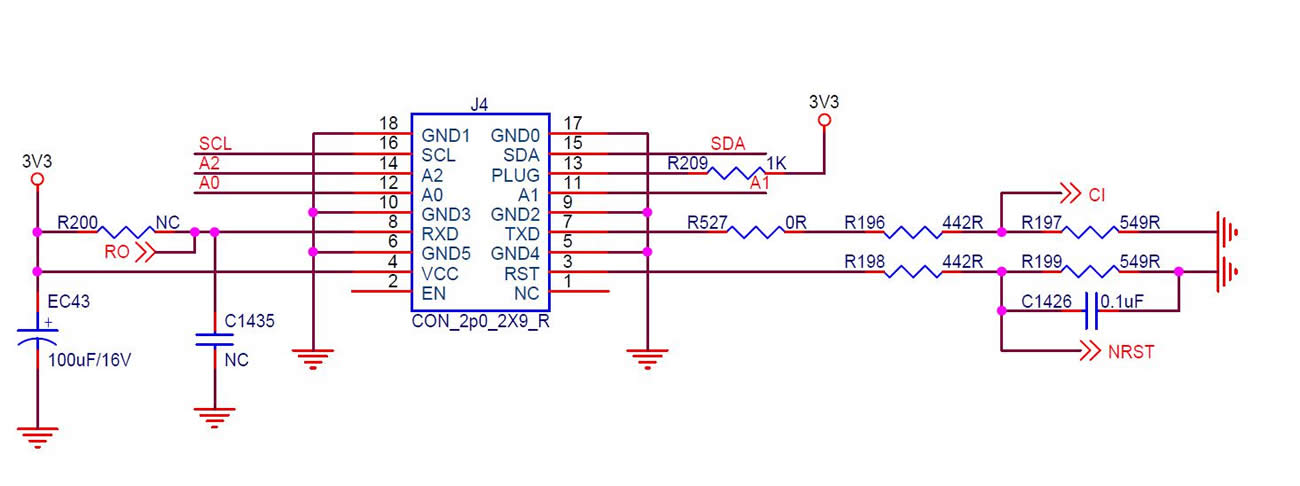
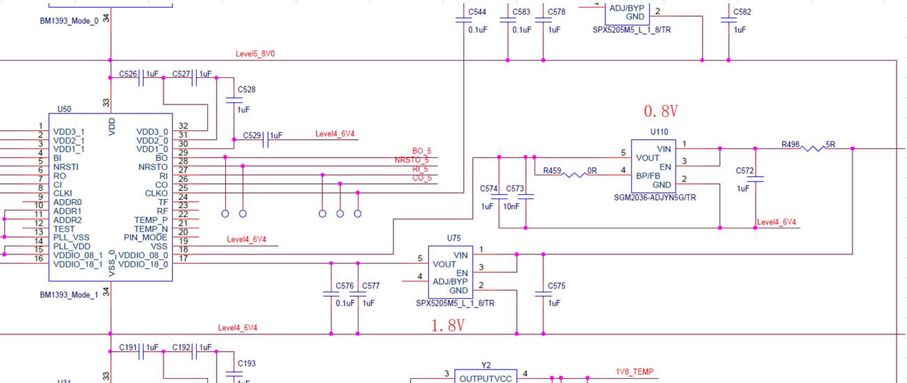
2.2.10 0.8V, 1.8V circuit schematic diagram
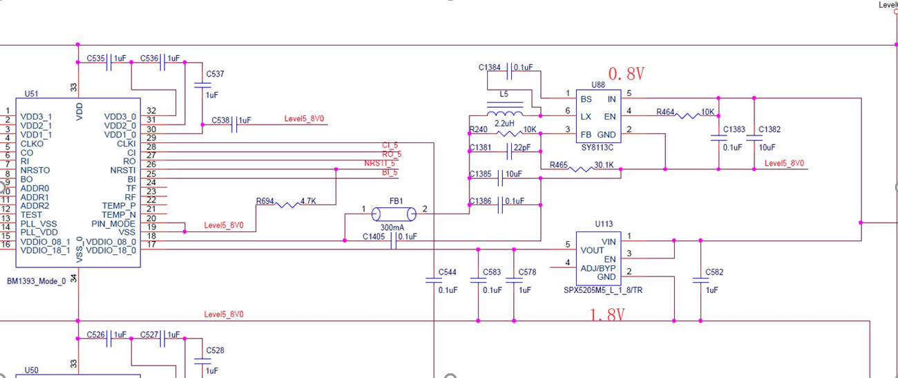
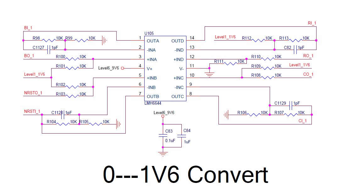
2.2.11 Schematic diagram for Level signal conversion
2.2.12 Schematic diagram for Y1, Y2 crystal oscillator

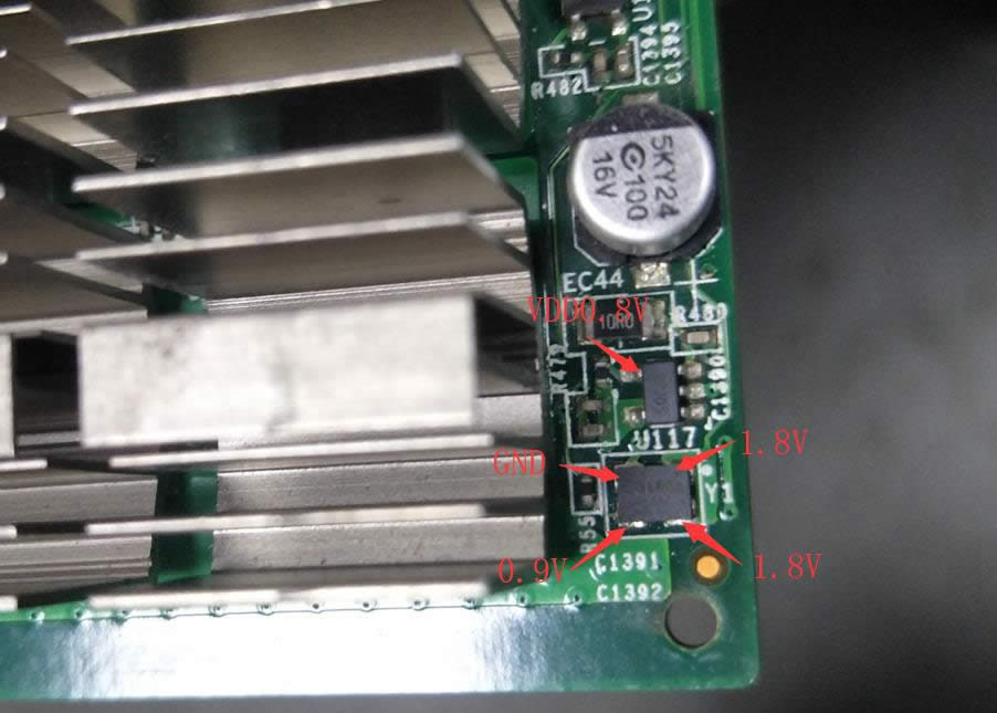
2.2.13 LDO 0.8V, 1.8V and crystal oscillator measurement
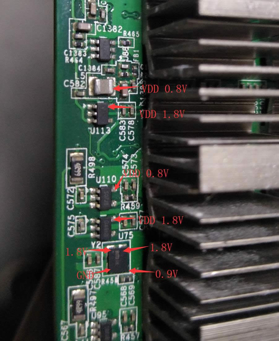
S9K S9SE maintenance ideas
During the maintenance, conduct 10 tests before and after the main test chip (five before and after the chip: CLKO, CO, RI, BO, NRSTO); DC-DC output and PIC voltage
CORE voltage; LDO (0.8V 1.8V), PLL-0.8V.
Detection method:
1. When the IO line is not inserted and only 12V is inserted: the DC-DC output is about 0V, and the boost output is about 0V. The PIC power supply of 3.3V must be powered. The other test voltages are all 0;
2. When the IO line is inserted and the test button is not pressed, there is no voltage output from DC-DC and boost. After pressing the test button, the PIC starts to work. At this time, the DC-DC outputs the voltage set by the test program of PIC jig, and boosts as it works. Then the jig outputs WORK, and returns to noce after computing. At this point, the normal voltage of each test point should be:
CLKO: 0.9V
CO: 1.6-1.8V, when the jig is just sent to WORK, since the CO is negative, the DC level will be lowered, and the instantaneous voltage is about 1.5V. RI: 1.6-1.8V, when the voltage is abnormal or too low during computing, the hash board will be abnormal or the hashrate will be zero.
BO: 0V when there is no computing, there will be a pulse jump between 0.1-0.3V during computing.
NRSTO: 1.8V. A reset signal is re-outputted each time the test button of the jig is pressed.
When the above-mentioned test point status or voltage is abnormal, please estimate the fault point based on the circuit before and after the test point.
Details and distinction of S9K S9SE chip’s configuration file

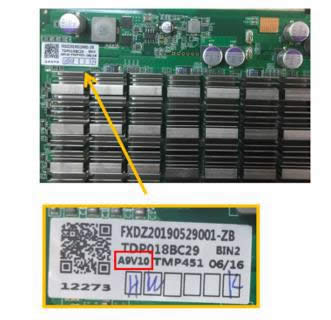
PCBA label diagram
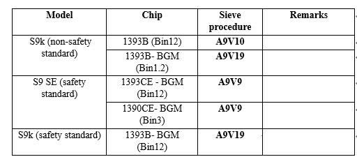

Description of chip correspondence
IV. Routine Maintenance Process

1. Routine testing: First carry out visual inspection of the hash board to be repaired to see if there is displacement, deformation, burning of small cooling fin? If there is such phenomenon, it has to be processed first; if the small cooling fin is displaced, remove it first and then clear the black adhesive, and then re-adhesive after repair.
Secondly, after it’s confirmed no problem visual inspection, the impedance of each voltage domain can be detected first to detect whether there is a short circuit or an open circuit. If found, it must be handled first.
Next, check whether the voltages in each voltage domain reach 1.6v, and the voltage difference between the voltage domains must not exceed 0.3V. If the voltage in a voltage domain is too high or too low, the circuits in the adjacent voltage domain generally have abnormal phenomena, and it needs to find the reason first.
2. After confirming there is no problem in the routine test (short circuit detection is necessary in routine test to avoid burning the chip or other materials due to short circuit when it’s power-on), a test box can be used for chip detection, and the detection results of the test box can be used to judge the location.
3. According to the result of the test box detection, start from the vicinity of the faulty chip, and detect the voltage of the chip test point (CLK IN OUT/RI IN OUT/CO IN OUT/BO IN OUT/NRST IN OUT) and LDO 0V8 1V8.
4. According to the signal flow direction, the RI signal is reversely transmitted (U60 to U1 chip), and several of the signals CLK CO BO NRST are transmitted forward (U1-U60), and an abnormal fault point is found through the power supply sequence.
5. When locating to the faulty chip, the chip needs to be rewelded. The method is to add a flux around the chip (preferably no-clean flux), heat the solder joints of the chip pins to a dissolved state, gently move up and down, left and right, and press the chip; promote the chip pins to joint the bonding pad again, collect the tin, so as to tin again. If the fault is the same after re-welding, the chip can be replaced directly.
6. After the repair of the hash board, the test box must be checked for more than twice. The time of the two tests: For the first time, after replacing the parts, the hash board needs to be cooled down; after passing the test, it is put aside first. For the second time, after the hash board is completely cooled after a few minutes, the test is performed. Although each of the two tests lasts only a few minutes, it does not affect the work. The repaired board is put aside, and the second board is repaired, after the second board is repaired, it is placed and cooled, then the first board is tested. In way, the repair is staggered and there is no delay in the total length of time.
7. For the repaired board, first it is necessary to classify the faults and record the replaced part model, location, and cause, to feed back to production, after- sales, research and development.
8. After recording, install the whole miner for normal aging.
V. Fault Type
Common fault types of the S9K S9SE hash board:
1. Cooling fin falls, shifts and deforms
The cooling fin on the PCB board on the back of the hash board chip is not allowed to shift or collide before power on, especially the cooling fin with different voltages. The contact of the cooling fins in different voltage domains means that there is a possibility of short circuit at different voltage points.
Moreover, determine that each of the cooling fin on the hash board has good heat conduction and is firmly fixed.
When replacing or re-installing the cooling fin, clean the residual adhesive on the cooling fin and chip and then coat again. The residual thermally conductive adhesive can be cleaned with absolute alcohol.
2. Impedance imbalance in each voltage domain
When the impedance of some voltage domains deviates from the normal value, it indicates that there are open and short circuits in the abnormal voltage domain. Generally the chip is the most likely to cause it. But there are three chips in each voltage domain, and often only one has problem when fault occurs. The method of finding the problem chip can detect and compare the ground impedance of test points of each chip to find the abnormal point.
If there is a short circuit, first remove the cooling fin on the same voltage chip, and then observe whether the chip pin’s tin is connected.
If a short-circuit point cannot be found on the appearance, search the short-circuit point according to the resistance method or current cut-off method.
3. Voltage imbalance in voltage domain
When the voltage in some voltage domains is too high or too low, there is usually an abnormal IO signal in the abnormal voltage domain or adjacent voltage domain, which causes the next voltage domain to work abnormally and the voltage to be unbalanced. The abnormal point can be found by detecting the signal and voltage of each test point, and some need to find the abnormal point by comparing the impedance of each test point.
Note that the CLK signal and the NRST signal are the two most likely to cause a voltage imbalance.
4. Lack of chips
The lack of chips means when the test box is being checked, not all of the 60 chips are detected, and often not all the chips are actually detected. The actually lost (undetected) abnormal chips are not in the displayed position. At this time, it is necessary to accurately locate the abnormal chip through testing.
The locating method can use the RI cutoff method to find the location of the abnormal chip. That is, ground the RI signal of a chip, for example, after the RI output of the 50th chip is grounded in the voltage domain, theoretically, if all the chips in the front are normal, the test box should display that 50 chips are detected. If not all 50 chips are detected, it means that the abnormality is before the 50th chip; if 50 chips are detected, it means that the abnormal chip is after the 50th chip. Use this dichotomy to find out where the abnormal chip is located.
5. Broken chain
A broken chain is similar to lack of chips, but in a broken chain, not all chips that cannot be found are abnormal, but all the chips after the abnormal chip are invalid due to a certain chip abnormality. For example, a chip itself can work, but it will not forward other chip information; at this time, the entire signal
chain will come to an abrupt end, and lose a large part of it, which is called broken chain.
The broken chain port information can be displayed. For example, when the test box detects the chips, only 30 chips are detected. If the number of preset chips is not detected in the test box, it will not run, so it will only display how many chips are detected, at this time, according to the displayed number "30", the problem can be found by detecting the voltage and impedance of each test point before and after the 30th chip.
6. No running
No running means that the test box cannot detect the chip information of the hash board, but displays NO hash board; this phenomenon is the most common and the fault range involved is also wide.
1) No running caused by abnormal voltage in a certain voltage domain; the problem can be found by measuring the voltage in each voltage domain.
2) A chip abnormality causes an abnormality that can be found by measuring each test point signal.
CLK signal: 0.9V; the signal is output from chip U1 chip to chip U60. In the current version, there are only two crystal oscillators, Y1 is transmitted from the first chip to the 30th chip, and Y2 is transmitted from the 31st chip to the 60th chip, and the CLKO signal is abnormally searched according to the direction of signal transmission.
CO signal: 1.8V; this signal is transmitted through chips U1, U2,,,,, U60, when a certain point in the binary method is abnormal, it can be detected forward.
RI signal: 1.8V; this signal is returned from chips U60,,,,,, U2, U1, confirm the cause of the fault through the chip signal trend; when S9K S9SE hash board does not run, the signal is the highest priority, first search for this signal.
BO signal: 0V, this signal can be lowered to high level when the chip detects that the RI return signal is normal, otherwise it is high level.
NRST signal: 1.8V; after the hash board is powered and the IO signal is inserted, the signal is transmitted from U1, U2,,,,, and U60 to the last chip.
3) LDO 0.8V, 1.8V abnormality maintenance
The normal value of the ground impedance of the LDO 0.8V IC output is 50-100 Ώ, and the normal impedance of the LDO 1.8V IC output is 0.9KΏ.
There are six LDO 1.8V single hash boards and twelve LDOs 0.8V (for example, the power supply of domain 1 U1-U10 is U61 LDO 1.8V , the power supply of U1-U5 is 0.8V U117, and the power supply of U6-U10 is 0.8V U79), Since the LDO is operated in series, the LDO ground short-circuit can be repaired by using the two-fifth method. First, take the middle chip, remove them one by one, and find the problem chip to replace it;
4) Single board Patter NG repair
Serial port print log (logo information), single-chip and whole-chip hash board none recovery rate needs to reach 98%, if noce response rate is lower than 98%, report Patter NG; according to serial port print log, give priority to the replacement of the chip with the lowest single chip noce recovery rate;
5) The whole miner J: 4 maintenance
1. J: 4 does not store the temperature sensing chip position, and needs to test with the test jig once, the temperature sending information is written into the EEPROM chip IC through the single board test jig;
2. The single board jig configuration file is wrong (the chip of the hash board, the BIN level does not match the jig configuration file), resulting in the whole miner reporting J: 4;
VI. Maintenance Instructions
1. During maintenance, the maintenance personnel must be familiar with the function and flow direction of each test point, the normal voltage value and the impedance value to ground.
2. Must be familiar with the chip soldering, so as not to cause PCB foaming deformation or pin damage.
3. BM1393 chip package, 16 pins on both sides of the chip. The polarity and coordinates must be aligned during soldering and must not be misaligned.
4. When replacing the chip, the thermally conductive fixing adhesive around the chip must be cleaned to avoid secondary damage of the chip caused by hanging or poor heat dissipation during IC soldering.
● Note:
1. Since the cooling fin on the back of the chip is connected to the chip, a special slender test lead must be used to detect the test point signal; apart from the metal exposed at the contact end, the other parts of the test lead must be sealed with a heat shrinkable tube so as to prevent the test lead from contacting with the cooling fin and the test point at the same time. In particular, the voltage difference between the upper and lower rows of circuit voltage is large, and will cause damage to the chip when contacting the ground (cooling fin) and test points in different voltage domains, and special attention shall be paid.
2. In soldering, since there are small cooling gins close to the PCB on the back of the chip, the heat conduction is fast. Therefore, it is necessary to use the bottom to assist heating (about 200 degrees) in soldering, which can improve the efficiency and reduce the damage to the PCB board. If there is no bottom heating device, remove the small cooling fin on the PCB on the back of the chip before replacing the chip.
Please contact our engineering department in time for new fault types. We will analyze and update this content continuously!
Дорогие клиенты,
Здравствуйте, с 1 по 5 мая 2026 года (GMT+8) в Китае отмечается День труда, и международная логистика будет приостановлена. Наша компания приостановит отгрузки во второй половине дня 30 апреля 2026 года и возобновит отгрузки со склада 6 мая (GMT+8). Приносим извинения за возможные неудобства. Спасибо за ваше понимание и поддержку.
С наилучшими пожеланиями,
ZEUS MINING CO., LTD.